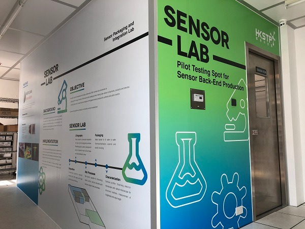
The Sensor Packaging and Integration Laboratory (Sensor Lab) is a dedicated hardware hub supporting full research and development processes of micro/nano sensors and associated devices, including sensor chip/devices fabrication and pilot runs, packaging, and testing.
Two locations equipped with Class 100/1000/10000 cleanroom space are offered to users for conducting research and product development. Apart from fully furnished cleanroom facilities, HKSTP and our partners also provide common wafer processing tools (including deposition, patterning, etching, packaging and characterisation), technical support and consultation services.
We also welcome R&D partners to formulate government-funded technology projects that would utilize the laboratory service as part of the pilot production.
Paper for Micro/ Nano sensors for healthcare and smart city
This paper provides a quick overview of sensor development at Science Park, followed by snapshots of the observations and insights of the speakers in 1st International Symposium on Micro/Nano Sensors for Healthcare and Smart City at December 10, 2018.
 Click to enlarge
Enquiry
- Sensor Lab User/ Partner Application
- Sensor Lab Visit
Information
Location:
Building 9W, 9 Science Park West Avenue
Operating hours:
9am to 6pm, Monday to Friday, except Hong Kong Public Holidays
Email:
Contact Us